專註於行業(yè)產(chǎn)品解決方案
專業(yè)研發(fā)精英團(tuán)隊,實力見證
免費(fèi)咨詢熱線:
13823783658專業(yè)研發(fā)精英團(tuán)隊,實力見證
免費(fèi)咨詢熱線:
13823783658免費(fèi)咨詢熱線:
13823783658
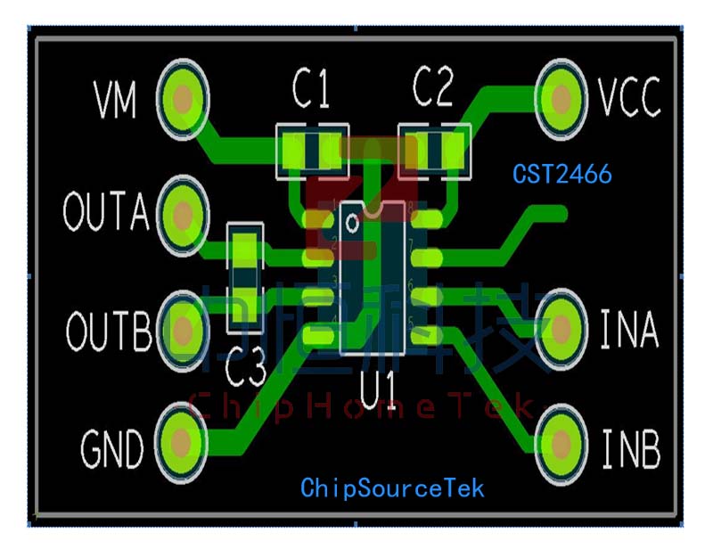


| Pin number | Pin name | I/O | Description |
| 1 | VM | -- | Motor power supply |
| 2 | OUTA | O | Motor drive output A |
| 3 | OUTB | O | Motor drive output B |
| 4 | GND | -- | Ground |
| 5 | INB | I | Logic input B |
| 6 | INA | I | Logic input A |
| 7 | NC | -- | No connection |
| 8 | VCC | -- | Logic power supply |
| Parameters | Symbol | Value | Unit | |
| Logic power supply voltage , VCC | VCC | 7 | V | |
| Motor power supply voltage , VM | VM | 11 | V | |
| Power dissipation | Pd | SOP-8 | 0.96 | W |
| Operating Temperature, Top | Topr | -20~85 | ℃ | |
| Junction temperature | Tj | 150 | ℃ | |
| Storage Temperature, Tstg | Tstg | -55~150 | ℃ | |
| Manual welding temperature | 350~370 | ℃ | ||
| Peak output current | Iop | 3.5 | A | |
| Continuous Output Current | Ioc | 2.1 | A | |
| PWM Frequency | fPWM | 33 | KHz | |
| Parameter | Symbol | Rating | Unit |
| Power supply voltage | VCC | 2.0~6 | V |
| Motor Power supply voltage | VM | 9.6 | V |
| High Input Voltage | VIN | 0.5xVCC | V |
| Low Input Voltage | VIN | -0.8~0 | V |
| Continuous Output Current | IOUT | -1500~1500 | mA |
| Parameter | Symbol | Test Condition | Min | Typ | Max | Unit |
| Overall Circuit | ||||||
| Standby Current | ICCST | INA=INB=GND | — | 1 | 5 | uA |
| Input control | ||||||
| High Input Voltage | VINH | 2 | 4 | 6 | V | |
| Low Input Voltage | VINL | — | — | 0.8 | V | |
| PWM Drive Frequency | FPWM | — | 20 | 33 | KHz | |
| Reverse brake Time Required | RVBT | from INA to INB or from INB to INA |
200 | 500 | — | uS |
| High Input Current | IINH | VIN=3V | — | 250 | 400 | uA |
| Low Input Current | IINL | VIN=0V | -1 | 0 | — | uA |
| Pull Down Resistor | RIN | — | 12 | — | KΩ | |
| Driving | ||||||
| Output Impedance(HS+LS) | RON | Io=±200mA | — | 0.26 | 0.6 | Ω |
| Protection Circuits | ||||||
| Thermal shutdown temperature | TTSD | Die temperature | — | 150 | — | ℃ |
| Input | Output | Function | ||
| INA | INB | OUTA | OUTB | |
| L | L | Hi-Z | Hi-Z | Stand-by(Stop) |
| H | L | H | L | A CH output |
| L | H | L | H | B CH output |
| H | H | L | L | Brake |
| 文件名稱: | 文件格式: | 立即下載: |
|---|---|---|
| 驅(qū)動線和1至14節(jié)鋰保資料 | ||
| 標(biāo)準(zhǔn)件2020彩頁 | ||
| CST2466 CST2466E | ||
| CST2466 CST2466E |
咨詢:CST2466/CST2466E
* 為必填項


